NICE
About Us
Research on Nanomaterial-based Integrated Circuits and Electronics (NICE) at DSU is an interdisciplinary research and education center focusing on semiconducting materials and devices design, modeling, fabrication and characterization.
Team Members with Expertise
NICE team members consist of faculty members from the area of material science, electrical engineering, physics, optics, chemistry and mathematics.
 |
Mukti Rana, Ph.D. Director and Principal Investigator of NICE & Professor of Engineering, Division of Physics Engineering, Mathematics and Computer Sciences mrana [at] desu.edu Website |
Research Interest and Expertise: Uncooled Infrared Detectors - Design and Fabrication, Materials for Uncooled Infrared Detection-Synthesis, characterization, 2-D Materials for Infrared Detection, 2-D and 3-D materials’ Interface, Ferroelectric and Pyroelectric Materials. |
 |
Jinjie Liu, Ph.D. Professor of Mathematics, Division of Physics, Engineering, Mathematics, and Computer Science, jliu [at] desu.edu Website |
Research Interest and Expertise: Numerical analysis and mathematical modeling of semiconducting and ferroelectric materials, Maxwell’s equations and the Schrödinger equation for electromagnetics, nonlinear optics, metamaterials, and semiconductor devices, second-harmonic generation (SHG) from metallic split-ring resonator (SRR), thin film, and peridynamic simulations of material fractures. |
 |
Yanan Xu, Ph.D. Assistant Professor of Mathematics, Division of Physics, Engineering, Mathematics, and Computer Science, yxu [at] desu.edu Website |
Research Interest and Expertise: Ferroelectric Materials Behaviors Modeling, Microbolometers Simulation, Semiconductor Materials Studies using Density Function Theory (DFT). |
 |
Mohammad Amir Khan, Ph.D. Professor, Division of Physics Engineering, Mathematics and Computer Sciences mkhan [at] desu.edu Website |
Research Interest and Expertise: Opto-electronic Based Sensors for Remote Sensing, Higher Harmonic Detection and Wavelength Modulation Spectroscopy, Mid- IR (Quantum Cascade laser) Technologies for the Environment and Health, Low Power Greenhouse Gas Sensor Systems and Sensor Networks. |
 |
Yuriy Markushin, Ph.D. Research Associate Professor, Division of Physics Engineering, Mathematics and Computer Sciences ymarkushin [at] desu.edu Website |
Research Interest and Expertise: Materials characterization; Attenuated total reflectance - Fourier transform infrared spectroscopy; Raman spectroscopy; Laser induced breakdown spectroscopy of materials; Uptake and distribution of nanoparticles and carbon nanotubes in plants; Immunoassay & lateral flow assays development. |
 |
Yanfeng Yue, Ph.D. Professor, Division of Physics Engineering, Mathematics and Computer Sciences yyue [at] desu.edu Website |
Research Interest and Expertise: Semiconductor nanocrystals (Quantum dots) for chemical sensing, Potentiometric sensors for environmental monitoring and remediation, Nanoporous carbons for energy storage and conversion. |
 |
Hacene Boukari, Ph.D. Professor, Division of Physics Engineering, Mathematics and Computer Sciences hboukari [at] desu.edu Website |
Research Interest and Expertise: Soft Matter Physics and Biophysics; Biotransport Phenomena in Complex Systems; Phase Transitions and Critical Phenomena; Optical Physics: Scattering (light, X-ray, neutron); Fluorescence; FTIR; LIBS; Raman; Imaging, Applications of Machine Learning in STEM disciplines. |
Related Grants
- “2D-3D materials’ development and their integration”, National Science Foundation, $200,000, Award Period: 09/2024-08/2026, DSU PI: Mukti Rana, Co-PI: Jin Jie Liu. Prime-Clarks Atlanta University.
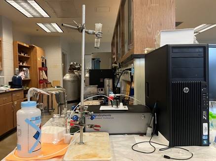
Facilities and Infrastructure
CHARACTERIZATION EQUIPMENT
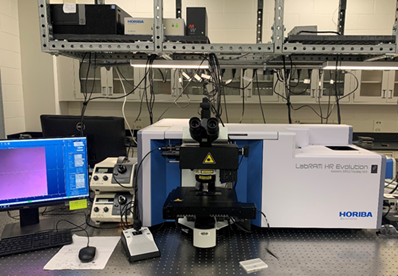
- Confocal micro Raman spectrometer (HORIBA LabRAM HR Evolution) for micro Raman and photoluminescence measurements. It also offers advanced confocal imaging capabilities in 2D and 3D. The laser excitations include 405 nm, 532 nm, 633 nm and 785 nm. The Raman spectrometer is also equipped with 532 nm low-frequency filters that enable the low-frequency Raman measurements down to 10 cm-1.
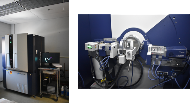
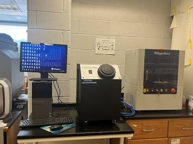
- Rigaku XRD Smart-Lab SE is a multipurpose X-ray diffraction system with intelligent guidance. The system is powered by Smart-Lab Studio ll to support the new architecture module platform. This ergonomic model allows the crossbeam optic module switches between Bragg-Brentano and parallel beam without changing optics. The HyPix-400 2D detector enables a seamless switch between 0D, 1D, and 2D detection modes depending on application type. The workflow integrated into the software enables fully automated measurement, including optics and sample alignment. These self-alignment optics maximize the time of use in the instrument and minimize the cost of ownership.
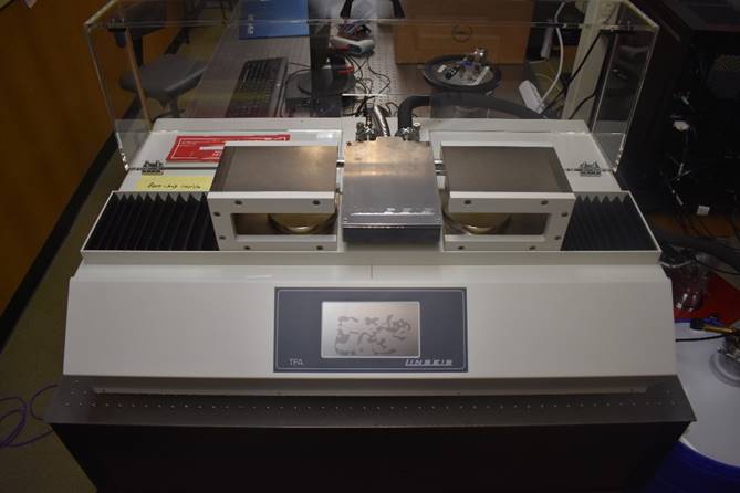
- Linseis thermal conductive measurement system consists of a measurement chamber, vacuum pump, primary sample holder with included heater, system integrated lock-in amplifier for measurement of thermal properties of thin films by 3ω-method. It has PC and LINSEIS software package including measurement and evaluation software. This equipment is optimized to measure thermal conductivity, specific heat, emissivity, electrical resistivity, and the See beck coefficient.
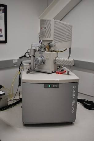
- Quanta FEG 250 Scanning Electron Microscope (SEM) and Scanning Transmission Electron Microscopy (STEM) is an environmental Scanning Electron Microscope used for high-resolution imaging and composition analysis by energy-dispersive X-ray microanalysis (EDS). The FEG column in Quanta 250 allows beam deceleration, which permits a resolution of 1.4 nm even at 1 kV electron landing voltage. STEM can be used for TEM samples on grids . This is a scanning TEM.
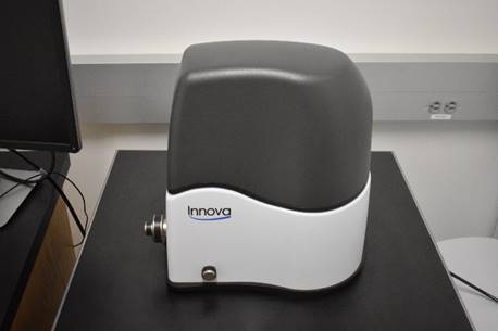
- Bruker Innova Atomic Force Microscope (AFM) is used for study the topography of material without direct contact. Using the disturbance in the layer that is reflected in the probe tip is interacting with the atomic force we could have an indirect Image of high quality of the subject of study.
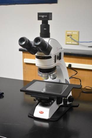
- Motic Panthera Microscope compact Epi illuminator carries a slot for polarizer and analyzer, ready for polarization contrast and to reduce internal reflections. The illuminator also includes the controls for varying the incident light in terms of mode (BF or DF) and illumination angle. The extended 22mm Field of View (FOV) offers 21% more visual area in comparison to a basic 20mm FOV system. The beam split of the trinocular versions (25° viewing angle) is fixed by 50/50 (vis/photo).
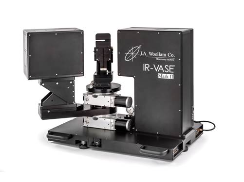
- J. A. Woollam Infrared VASE Ellipsometer: This will work for all types of materials, including semiconductors, dielectrics, polymers, metals, multi-layers, and more. It has Variable wavelength and angle of incidence enable flexible measurement capabilities. This has the unique features include angle of incidence range from 32 to 90 degrees and spectral range from 1.7 to 30 microns. This is capable of changing the temperature between 150K to 320K.
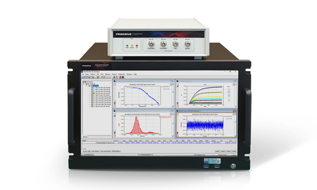
- Low Noise measurement System: The Low noise amplifier is made by Premarius (9813DXC) and it is a very unique low noise low frequency amplifier with the associated data acquisition system. The instrument has the following unique characteristics than any of the systems used in the world. It is a low noise Pre-amplifiers integrated into one unique system. It has minimum DC current resolution: <0.1nA (For HPcLNA), ~0.1uA (For cLNA & vLNA). The typical noise measurement speed (Highest speed): <10 sec/bias. The Built-in ADC and DSA are Bandwidth: >10MHz and Resolution: 16 bit. The RTN measurement is to maximum 960K points. It has a wide impedance range: 10 to 10 MOhms.
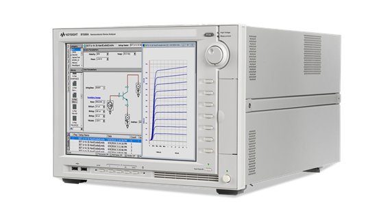
- Keysight Device Parameter Analyzer B1500A: The Keysight B1500A semiconductor parameter analyzer is an all-in-one device characterization analyzer designed for comprehensive semiconductor testing. This versatile instrument supports various measurement techniques, including IV, CV, pulse/dynamic IV, and more, making it an ideal choice for semiconductor testing applications. The mainframe and plug-in modules offer unmatched flexibility, enabling the characterization of various electronic devices, materials, semiconductors, active/passive components, and more.
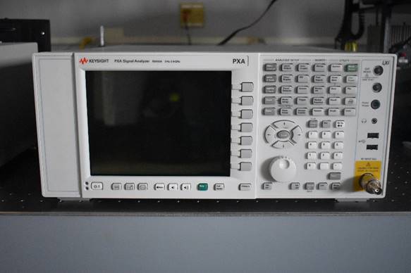
- Keysight PXA Signal Analyzer N9030A provides frequency coverage up to 50 GHz. The PXA signal analyzer delivers exceptional performance that reduces measurement uncertainty and reveals new levels of signal detail, starting with up to 75 dB spurious-free dynamic range at the 140-MHz analysis bandwidth. Industry-leading specifications include –129 dBc/Hz phase noise (room temperature) at 10 kHz offset (1 GHz), ±0.19 dB absolute amplitude accuracy, and sensitivity of –172 dBm displayed average noise level (DANL) at 2 GHz (with preamplifier and Noise Floor Extension technology).
- AixCCT TF 2000E thin film analyzer for measuring ferroelectric, piezoelectric and pyroelectric properties of thin film. The FE module consists of a voltage amplifier for output voltages of up to 30 V and current amplifiers for detecting the test current. Multiple ranges between 10 pA and 1 A are available in order to make full use of the bandwidth and definition.
- Oriel MS257 Monochromator is a completely automated instrument with enough versatility to satisfy most spectroscopy applications. It is an F/3.9 instrument with a focal length of 257.4 mm, usable as a monochromator or true flat field imaging spectrograph. Stray light is negligible, and there are no re-entrant spectra. The MS257 has two output ports, one input port, and support four gratings.
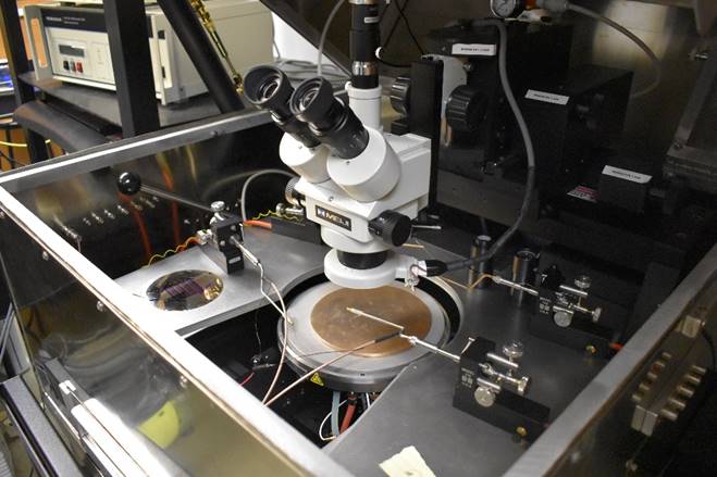
- Micromanipulator - 450PM Manual Probe Station is a high-efficiency general-purpose manual analytical probe station. It has a microscope and a variable temperature chuck associated with it. The temperature of the variable temperature chuck can be varied between 250 K to 320 K.
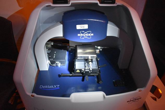
- Bruker DektakXT profilometer is used for measuring thin films’ thickness, stress, surface roughness, and form in various areas
- West Bound Bonding machine 7374E is used for bonding the devices by ultrasonic wire bonding method.
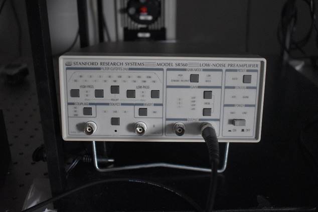
- SR560 Low noise amplifier from Stanford Research is a high-performance, low-noise preamplifier ideal for a wide variety of amplification, including low-temperature measurement and optical detection.
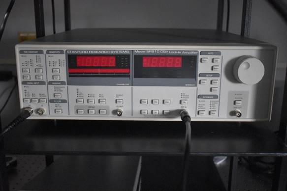
- SR810 DSP Lock-In Amplifier from Stanford Research provides high performance measurements using digital signal processing (DSP) to replace the demodulators, output filters, and amplifiers found in conventional lock-ins. The range of operation of these devices is from 1mHz to 102 kHz and 100 dB of drift-free.
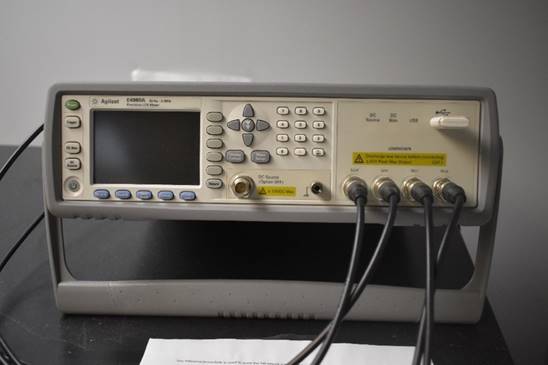
- Agilent E4980A LCR Meter provides the best combination of accuracy, speed, and versatility for a wide range of component measurements. Offering fast measurement speed and outstanding performance at both low and high impedance ranges. The E4980A is a tool for general R&D and manufacturing tests of components and materials.
- AlliedHitech Multiprep system 8: Capabilities include parallel polishing, angle polishing, site-specific polishing or any combination thereof. It provides reproducible results by eliminating inconsistencies between users, regardless of their skill. Samples such thin film depositions, metalized layers on PCB and various microchip substrates can all be cross sectioned, polished, ground. Including face polishing and edge polishing.
- Buehler Ecomet 3 and Automet 3 power grinder and polisher: This is designed to work for bulk and larger samples mostly embedded in epoxy resins for sample holding and support. It can also be used for metallurgical and geological sample perpetrations.
- Quorum Q150R plus Rotary Pumped coater: Au/Pb coating, Carbon Coating and Glow-discharge for TEM Grids
- Reichert-jung UltraCut E ultramicrotome: Used mostly for ultramicrotomy of biological samples but can be used for ultrathin sectioning of soft materials, plastics and polymers for ultra internal structure analysis on TEM and SEM.
- The phase purity of the semiconductor nanomaterials will be characterized by using X-ray diffractometer (Rigaku Miniflex 600).
- Electrospinner for lab-scale electrospinning of nanofiber (NE200 Electrospinning/Spraying Machine) to prepare precursors for 2D semiconductors.
- Model 660 series electrochemical analyzer/workstation for electrochemical evaluations.
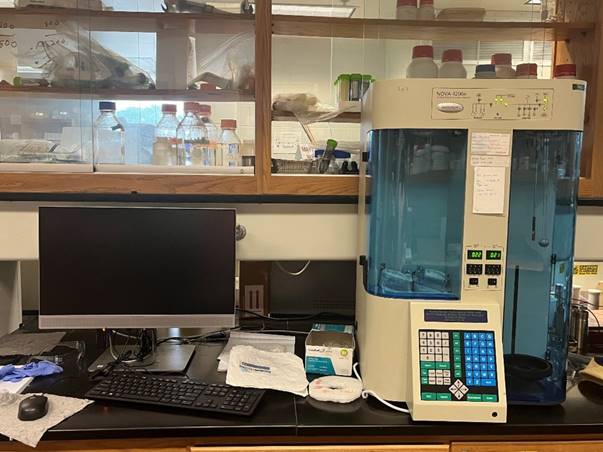
- BET analyzers (ASAP 2020 and NOVA 4200e) will be used to check the surface areas and pore volume for resultant semiconductor nanomaterials (QDs).
- Raman confocal Horiba XplorRA
- Optical: Leica DM 5000B TCS-SP5 upright optical Microscope. Equipped for multicolor acquisition (up to 4 channels). 405, 457, 477, 488, 514, 532 and 633 nm laser excitation lines.
- Optical: Olympus IX71 inverted inverted microscope for widefield and DIC microscopy. It is equipped with high sensitivity camera (Photometrics QuantEM 512C), computer-controlled Prior motorized stage, Metamorph software, diverse cubes, high-NA objectives.
- Optical: Olympus upright BX53, polarizing microscope which is equipped with a Q-imaging camera.
- Optical: Zeiss LSM 510 confocal microscope equipped with with Argon/Krypton 488/568 and HeNe 633 lasers.
- Optical: NIKON SMZ-18 Zoom Stereo Microscope for epi-fluorescence and dark-field microscopy. It is equipped with a DS-Qi2 monochrome CMOS camera and TokaiHit temperature-controlled stage.
- Spectrometer: ISS K2 phase + modulation spectrometer for fluorescence spectroscopy and fluorescence anisotropy. It is equipped with a 300 W xenon arc lamp, a 484-nm laser diode, and two LEDs at 280 and 370 nm; a monochromater from 200 to 1200 nm range and a ± 0.2 nm wavelength accuracy.
- Spectrometer: Varian Cary 100 BIO spectrometer for UV-visible light for absorbance and transmittance measurements.
Spectrophotometers:
- Bruker Raman Verification Optics Analyzer (Bruker)
- Nanodrop Spectrophotometer 2000 (Thermo Scientific Corporation)
- Nanodrop Fluorospectrometer 3300 (Thermo Scientific Corporation)
- Nicolet 6700 Fourier Transform Infrared Spectrophotometer (Thermo Scientific Corporation)
Chemical Equipment:
- ESEQuant LR3 Lateral Flow Readers (Dialunox)
- Differential Scanning Calorimetry Instrument Q200 (TA Instruments)
- 80C Ultra Low freezer.
- Yamato Spray Dryer ADL-310.
- IKA Rotary Evaporator RV 10.
- IKA Ultra-Turrax Homogenizer.
- VorTemp 56 Shaking Incubator.
- Milli-Q A-10 water purification system.
- Refrigerator, centrifuges, incubator, pH meters, micro-plate readers, polymerase chain reaction (PCR) thermocyclers, gel electrophoresis, analytical precision balances, shakers, vacuum pumps, micro-pipettes, necessary labware and sample preparation room.
- Gas chromatography thermo-conductivity detector (GC-TCD),
- Photochemical reactor (Rayonet RPr 200), contact angle goniometer (Ossila, L2004A10),
- Home-made two-compartment electrochemical cell
- Two Model 660 series electrochemical analyzer/workstation and potentiostat (Pine Research AFCBP1) for electrochemical evaluations.
- Thermal gravimetric analysis (TGA) (Perkin Elmer Pyris Diamond),
- Lab planetary micro mill (Fritsch Pulverisette 7), atomic force microscopy
- FT-IR (Shimadzu IRPrestige-21), high pressure adsorption analyzer (VTI HPVA-100)
- Absorption kinetic analyzer (house-built)
- Inductively coupled plasma mass spectrometry (ICP-MS) (Agilent 7900)
- High-performance liquid chromatography (HPLC) (Agilent 1100)
- Nuclear magnetic resonance spectrometer with temperature controller (NMR) (Oxford AS 400).
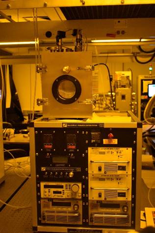
DEPOSITION AND PROCESSING EQUIPMENT
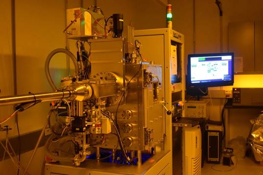
- The Torr Magnetron Sputtering Deposition With this system, we could sputter two metals simultaneously using RF guns.
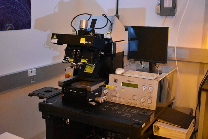
- MA6 Mask Aligner is primarily used to expose photo-definable materials. It has the capability to use 4” wafers.
- Kurt J Leskar PRO Line PVD 75 sputtering system is the next generation thin film deposition system based on the workhorse PVD 75 platform. A few of the key advantages offered in this innovative, best-of-class design are a technically superior chamber design, an industry-best software control system with advanced programming capability, automatic substrate loading, and numerous features for optimized thin film performance.
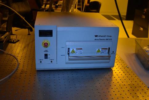
- W Allwin21 AccuThermo AW 610 is a rapid thermal processing (RTP) system that uses high-intensity visible radiation to heat single wafers for short process periods at precisely controlled temperatures. Combined with the heating chamber’s cold-wall design and superior heating uniformity, these capabilities provide significant advantages over conventional furnace processing.
- Plasma Asher is used to remove the photoresist or other sacrificial layers for various device applications.
- Specialty coating System 6800 Spin Coater enables to develop and refine coating applications efficiently and accurately.
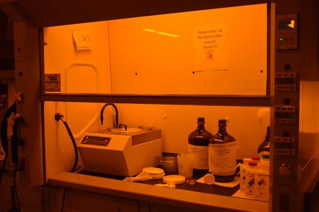
- Acid and Solvent hood is the workplace to develop the microfabrication chemical process.
SIMULATION AND COMPUTATIONAL CAPABILITIES
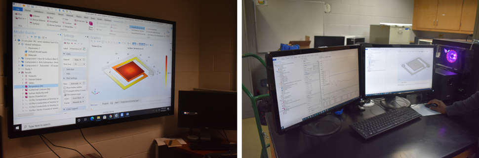
- COMSOL Multiphysics software is installed in two computers in our lab to design and simulate various sensors and devices. This simulation software helps to understand, predict, and optimize real-world designs, devices, and processes. COMSOL Multiphysics is a simulation platform that provides fully coupled Multiphysics and single-physics modeling capabilities. The Model Builder includes all of the steps in the modeling workflow — from defining geometries, material properties, and the physics that describe specific phenomena to solving and postprocessing models for producing accurate results.
- EXXACT GPU-based Server for mathematical simulations and machine-learning modeling.
- Data Visualization laboratory.
Relevant Publications
- “Effects of post-transfer annealing and substrate interactions on the photoluminescence of 2D/3D monolayer WS2/Ge heterostructures”, Tianyi Zhang, Andrew Voshell, Da Zhou, Zachary D. Ward,e Zhuohang Yu, Mingzu Liu, Kevin O. Díaz Aponte, Tomotaroh Granzier-Nakajima, Yu Lei, He Liu, Humberto Terrones, Ana Laura Elías, Mukti Ranac and Mauricio Terrones, Nanoscale, Issue 29, July, 2023. https://pubs.rsc.org/en/content/articlepdf/2023/nr/d3nr00961k
- “High Responsivity a-SixGe1-xOy:H Microbolometers”, Mukti M. Rana and Donald P. Butler, IEEE Sensors Journal,vol. 7, no. 10, October, 2007, Pages 1413-1419.
- “Magnetron Sputtered Lead Titanates Thin Films for Pyroelectric Applications: Part 1: Epitaxial Growth, Material Characterization”. Materials 2024, 17, 221. https://doi.org/10.3390/ma17010221
- J. Liu, S. Appiah-Adjei, and M. Brio, Iterated Crank–Nicolson Method for Peridynamic Models, Dynamics, 4, 192–207, 2024.
- J. Liu, J. Cornelius, and M. Brio, FDTD Method with Explicit Non-iterative and Second Order Treatment for Kerr Nonlinearities, IEEE Journal on Multiscale and Multiphysics Computational Techniques, 7, 195-199, 2022.
- “Electro-thermal numerical analysis of microbolometer over various kinds of design structure under adjustable thermal conductance in the Microeletromechanical system”, Yanan Xu, Mukti Rana, Kevin Diaz-Aponte. Heliyon, 2023 Mar 24; 9(4): e14886. DOI: 10.1016/j.heliyon.2023.e14886.
- “Design and Simulation of Microbolometer with Dual Cavity for High Figure of Merits”, Kevin Diaz-Aponte, Yanan Xu, Mukti Rana. Micromachines (Basel), 2023 Apr 27; 14(5): 948. DOI: 10.3390/mi14050948.
- “2D-Modeling for the temperature composition dependent thermal-conductivity of AlmNn compounded semiconductor materials”, Yanan Xu, Mukti Rana, Matthew C. Tanzy. Materials Research Express, 7(6), 065901, 2020.
- M. Brio, J.-G. Caputo, K. Gwirtz, J. Liu, and A. Maimistov. Scattering of a short electromagnetic pulse from a Lorentz–Duffing film: Theoretical and numerical analysis, Wave Motion, 89, 43-56, 2019.
- A. Safi, J.E. Landis, H.G. Adler, H. Khadem, K.E. Eseller, Y. Markushin, S. Honarparvaran, A. De Giacomo, N. Melikechi. (2024) Enhancing biomarker detection sensitivity through tag-laser induced breakdown spectroscopy with NELIBS. Talanta. 271, 125723.
- F. Candan, Y. Markushin, G. Ozbay. (2022) Uptake and Presence Evaluation of Nanoparticles in Cicer arietinum L. by Infrared Spectroscopy and Machine Learning Techniques. Plants (Basel). 11, 1569.
- N. Melikechi, Y. Markushin. (2022) Tag-laser-induced breakdown spectroscopy with Si, Ti, and Fe micro-particles and analysis of leptin in a phosphate buffer solution, Spectrochimica Acta Part B: Atomic Spectroscopy, 188, 106357.
- Douglas Austin, Jared Carney, Dale K. Hensley, Jihua Chen, Brianna E. Altidor, Zhiyong Guo, Elizabeth Michaelis, Mariana K Kebaso, Yanfeng Yue, “Sulfur Functionalized Biocarbon Sorbents for Low-Concentration Mercury Isolation”, Dalton Trans., 2024, 53, 2098.
- Jared B. Carney, Shannon M. Mahurin, Yuying Zhang, Yaping Wang, Gerald Poirier, Yong Zhao, Douglas Austin, Elizabeth Michaelis, Yanfeng Yue, “High Porous Biocarbon Monoliths for Methane Storage”, Microporous Mesoporous Mater., 2023, 112921.
- Changsheng Shan, Xi Feng, JingxuanYang, Xu Yang, Hong-Yu Guan, Monica Argueta, Xing-Long Wu, Dao-Sheng Liu, Douglas J. Austin, Ping Nie and Yanfeng Yue, “Hierarchical Porous Carbon Pellicles: Electrospinning Synthesis and Applications as Anodes for Sodium-Ion Batteries with an Outstanding Performance”, Carbon, 2020, 157, 308.
- High-precision characterization of quantum-cascade laser frequency response using wavelength modulation spectroscopy, MH Hlaing, C Azevedo, MA Khan, Review of Scientific Instruments 95 (3), 2024.
- Precision spectral line-resolution to classify greenhouse gas species in broadband mid-infrared sensing, Z Juracka, Z Juracka, A Khan, 2023 Conference on Lasers and Electro-Optics (CLEO), 1-2, 2023.
- Mid-infrared broadband sensing and temperature dependence of trace gas molecular transitions, A Alexis, Z Juracka, EK Ibrahim, MA Khan, Photonic Instrumentation Engineering X 12428, 164-170.
- L. W. Simpson, G. L. Szeto, H. Boukari, T. A. Good, and J. B. Leach, “Collagen Hydrogel Confinement of amyloid-b Accelerates Aggregation and Reduces Cytotoxic Effects” Acta Biomaterialia 112, 164-173 (2020). https://doi.org/10.1016/j.actbio.2020.05.030.
- A. Bhat, K. Huan, T. Cooks, H. Boukari, and Q. Lu. “Probing Interactions between AuNPs/AgNPs and Giant Unilamellar Vesicles (GUVs) Using Hyperspectral Dark-field Microscopy,” Int. J. Mol. Sci. 2018, 19(4), 1014; doi:10.3390/ijms19041014.
- DM. Surmick, H. Boukari, J. Woodward, AC Stowe, and N. Melikechi. “Uncertainty of Integrated Intensity Following Line Profile Fitting of Multiline Spectra,” Appl Spectrosc. (2018) 1:3702818756652. doi: 10.1177/0003702818756652; PMID 29336588.
Contact
Mukti Rana, Ph.D.
Director and Principal Investigator of NICE &
Professor of Engineering, Division of Physics Engineering,
Mathematics and Computer Sciences
Delaware State University
Dover, DE 19901
302.857.6588
mrana [at] desu.edu
Relevant patents
- “Germanium Tin Oxide Thin Films For Uncooled Infrared Detectors”, Investigators: Mukti Rana, and Jaime Cardona, Patent Number: 10337927, Date of Patent - July, 2019.
- “Germanium tin oxide thin films for uncooled infrared detection, Investigators: Mukti Rana, and Jaime Cardona, Patent number: 10840399, Date of Patent - November, 2020.
- “Medium Wave Infrared (MWIR) and Long Wavelength Infrared (LWIR) Operating Microbolometer with Raised Strut Design”, Investigators: Mukti Rana and Andrew Voshell, Patent Number-10483416, Date of Patent - November, 2019.
- “Germanium Silicon Tin Oxide Thin Films For Uncooled Infrared Detection”, Investigators: Mukti Rana, Larine Mbabit and Nibir Dhar, Patent number: 10704959. Date of Patent - July, 2020.
- Y. Markushin. Enhancement compositions and uses thereof. Patent Application: 63/320,758, 2022, PCT/US2023/015474, 2023.
Group Pictures